Besides it’s abundance in lithosphere, one of the key reasons why silicon has become the dominant semiconductor is that SiO2, the native oxide counterpart of silicon can be highly dense, uniform and insulative, while forming a very high-quality interface with silicon itself. Synthesized simply by heating silicon wafer in oxygen atmosphere, SiO2 is widely used as the gate dielectric of transistors, the passivation layer of chips, the protective barrier for diffusion doping as well as many other functional components in all kinds of nanoelectronics devices. No other semiconductors (e.g. Ge, SiGe, GaAs, InP, CNT, 2D MoS2 and WSe2) possess such high-quality native oxide like SiO2. However, with the mainstream CMOS processing approaching sub-5 nm node, it became increasingly clear that Si/SiO2 system is coming to an end, as SiO2 has a far too low dielectric constant (ε = 3.9). In order to extend Moore’s Law, it is most urgent to find the combination of ultrathin high-mobility semiconductor and ultrathin high-κ (ε > 10) native oxide.

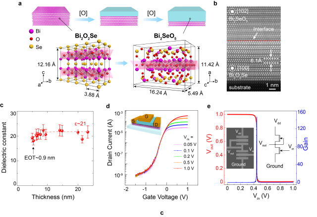
Fabrication of Bi2O2Se/Bi2SeO5 transistors and logic circuits.
Recently, a team led by Professor Hailin Peng at Peking University found the native oxide of high-mobility two-dimensional semiconductor embodies both high interfacial quality and large dielectric constant. This high-κ native oxide Bi2SeO5 shows excellent performance in 2D Bi2O2Se-based field-effect transistors and logic gates. Based on their previous research of high-mobility semiconductor Bi2O2Se (Nat. Nanotech. 2017, 12, 530; Nano Lett. 2019, 19, 2148), Peng’s group proposed that the intercalation of oxygen atoms between layers can transform Bi2O2Se into a wider bandgap material, Bi2SeO5 (bandgap from 0.8 eV to 3.9 eV). First-principle calculations further showed that these two materials and form a typical type I heterojunction with band offset at both CBM and VBM larger than 1 eV, which is most suitable for field-effect devices.
After several years’ exploration, Peng’s group successfully developed a complete process package based on 2D Bi2O2Se/Bi2SeO5, including controlled thermal oxidation of Bi2O2Se, selective etching and device fabrication. Cross-sectional TEM image shows the atomically sharp interface between Bi2O2Se and Bi2SeO5. C-V measurements as well as microwave impedance microscopy both confirmed the ultra-high dielectric constant of Bi2SeO5 (ε ~ 21). Field-effect transistors are fabricated with regional-selective etching and microfabrication techniques, showing carrier mobility > 300 cm2V-1s-1, Ion/Ioff ~ 106, near-ideal subthreshold swing (SS < 75 mV/dec) as well as much reduced transfer curve hysteresis. Most importantly, effect oxide thickness (EOT) of these FETs can be as small as 0.9 nm, with gate leakage much smaller than thermal SiO2 of similar EOT. The inverter circuits constructed by these FETs have a maximum voltage gain >150 at Vdd = 1 V.
To conclude, two-dimensional Bi2O2Se/Bi2SeO5 is the first integration of semiconductor and native high-κ gate oxide. Combined the ultra-thin planar structure of 2D materials and their natural resistance to short-channel effect, this material system can break through the bottleneck of modern electronic industry, and hopefully extend Moore’s Law.

Figure (a) Step-by-step oxidation of 2D Bi2O2Se. (b) Spherical aberration-corrected cross-sectional TEM of Bi2O2Se/Bi2SeO5 heterostructure. (c) Thickness-dependent dielectric constant of Bi2SeO5. (d) Transfer curves of Bi2O2Se/Bi2SeO5 field effect transistors. (e) Measurements of inverter circuits.
This article was published online by Nature Electronics on July 27, 2020, entitled “A native oxide high-κ gate dielectric for two-dimensional electronics” (DOI: 10.1038/s41928-020-0444-6). Prof. Hailin Peng at College of Chemistry and Molecular Engineering, Peking University is the corresponding author of this article. The first author Tianran Li and Teng Tu at Peking University contributed equally to this work. Other collaborators include Prof. Peng Gao at Peking University, Prof. Binghai Yan at Weizmann Institute of Science, and Prof. Keji Lai at the University of Texas at Austin.
This work was financially supported by the National Key Research and Development Program of China, the National Natural Science Foundation of China, and Beijing National Laboratory for Molecular Sciences.